X-ray photoelectron spectroscopy is a surface-sensitive spectroscopy technique which provides valuable quantitative and chemical state information from the material being studied. This technique is based on the Photoelectric Effect. When a material is irradiated with x-rays, photoelectrons are subsequently ejected from atoms in the near surface. The kinetic energy of an emitted photoelectron is equal to the difference between the photon energy, and the binding energy of the electron (K.E. = hν - B.E.). The technique is inherently surface sensitive because the x-ray energy is low (‹1,500 eV). The majority of the signal detected originates from the outer 1-10 nm of a sample. The spectra contain information about the elemental composition, concentrations and chemical environments (i.e. oxidation states) of surface and near surface atoms. The analyses are non-destructive for many, but not all materials.
Typical Applications
- Thin film and coatings
- Surface functionalization
- Polymers and adhesives
- Mineralogy, geochemistry, and petrochemistry
- Metallurgy
- Catalysis
- Microelectronics and semiconductors
- Surface characterization of solids.
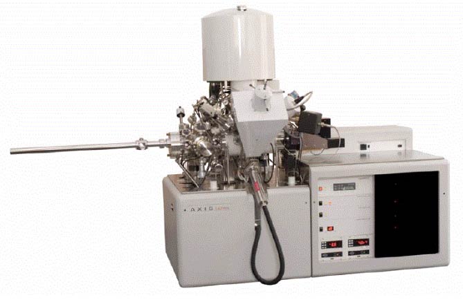
Kratos Axis Ultra DLD
With fast measurement speed and push-button operation, the alpha-SE is ideal for qualifying thin films. Single-layer dielectrics on silicon or glass substrates can be measured in seconds. Log results for easy-to-use comparisons in both graphical and tabular formats. Advanced models provide quick and efficient fits for a wide variety of materials you may encounter. Patented technology allows accurate measurements on any substrate: metal, semiconductor, or glass. On transparent substrates, the alpha-SE measures depolarization to correct for light returning from the backside of the substrate. This unwanted light can confuse other ellipsometers, but the alpha-SE ensures accurate optical constants.
System details:
- Capabilities:
- Single-point spectra
- Line profiles
- Area chemical maps
- Depth profiles
- UPS
- X-ray Source:
- Monochromatic Al Kα (1.486 KeV)
- Non-monochromatic dual anode Al Kα and Mg Kα (1.253 KeV)
- Sputter Source: Ar+ ion gun with ion energy selectable from 500 to 4000 eV
- Analysis Area (spot size):
- Hybrid mode: 700x300 μm
- Small spot modes: 15, 27, 55, 110 μm
- Imaging: predetermined analysis areas of 200, 400, 800 μm, and 2 mm
- Detection Limits:
- Sensitive to elements with Z ≥ 2 (all elements except for H and He)
- Typical minimum detectable concentrations: 0.1 – 1 % (atomic)
- Typical qualification error: 10 %
- Resolution (imagining): 3 μm
- Maximum Sample Dimensions By Mounting Method (width x length x thickness):
- Stub: 25 x 40 x 4 (mm)
- Standard Bar: 24 x 100 x 4 (mm)
- Constant Height Bar: 25 x 30 x 8 (mm)
Location: FH208